
Eulitha makes lithography equipment and solutions for photonics manufacturing. Established in 2006, Eulitha has been building new tool platforms and discovering innovative patterning solutions to match developing market needs. Built around IP-protected Displacement Talbot lithography, Eulitha's solutions are reliable and low cost for high-resolution patterning.

DTL(Displacement Talbot Lithography)
Eulitha's Displacement Talbot Lithography (DTL) is a new paradigm in optical lithography. It leverages the properties of light diffracted by a periodic pattern on a mask to print periodic nanostructures with unparalleled resolution and precision in a non-contact configuration.
In a DTL exposure, a periodic mask is illuminated by a coherent light source, such as a laser. This illumination produces a intricate interference pattern between the mask and substrate planes. During exposure, a substrate with photosensitive material displaces, or moves through the interference pattern, patterning the desired nanostructures with exceptional accuracy.
The process of integration by the substrate movement creates an extremely large effective depth of focus which is many orders of magnitude larger than projection tools with comparable resolution. This is particularly useful when patterning on topography, curved surfaces, or substrates that struggle with flatness.
Eulitha offers a variety of optical lithography tools purpose-built to take advantage of the DTL concept. The range of tools includes different wavelength choices such as i-line and DUV wavelengths depending on resolution needs of the application, manual R&D systems and fully automated high volume manufacturing systems.
Advantages
Low-cost, high-resolution patterning (~60nm min critical dimension)
Large exposure fields
- 140mm x 140mm imageable area (with 6in standard mask)
- Seamless device printing
- No complex reduction/magnification optics
Very large depth of focus
- Patterning on surfaces that are non-planar, topography, curved, etc.
- Up to millimeters of depth of focus (DOF)
Mask-locked design
- Tight pitch control (> 2 pm)
- Single-exposure design can have different patterns, pitches, duty cycles, and orientations
Reliable, repeatable patterning

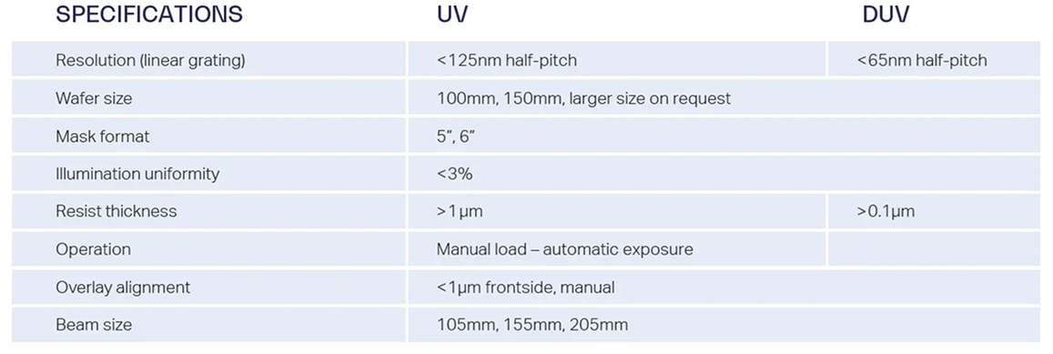
PhableR
Designed for research and development applications, the PhableR lithography tool offers high-resolution printing of periodic structures in an affordable and compact tabletop system.
Utilizing displacement Talbot lithography technology, sub-micron pitch periodic structures are printed with high uniformity and fidelity. The PhableR is a manually operated system.
The PhableR is a single exposure field platform available in UV and DUV sources and various beam sizes.
Applications
ACADEMIC (R&D)
- Nano Optics
- Nano Materials
- Plasmonics
- Research & Development
XR (AR/VR/MR)
- Near-Eye Waveguides
- Head-up Displays (HUD)
OPTOELECTRONICS
- DFB/DBR Lasers
- VCSEL Polarizer Gratings
- PCSEL Photonic Crystals
- Nanowire Devices
OPTICAL COMPONENTS
- Telecom Gratings
- Anti-Reflective Surfaces
- Laser Diffraction Gratings
- Spectrometer Gratings
- Wire Grid (Polarizer)
BIO/MEDICAL
- Bio Molecular Sensors
- X-Ray Imaging
COLOR/VISUAL EFFECT
- Structural Colors
- Security Applications

PhableX
The PhableX tool is a semi-automated lithography solution for photonics customers. The two port cassette design with transfer robot increases consistency and throughput. Automated wafer alignment and handling make the PhableX an operator-friendly platform. The PhableX is customizable with UV and DUV sources, 150mm and 200mm beam size, and various mask sizes.
Applications
OPTOELECTRONICS
- DFB/DBR Lasers
- VCSEL Polarizer Gratings
- PCSEL Photonic Crystals
- Nanowire Devices
- PSS
OPTICAL COMPONENTS
- Telecom Gratings
- Anti-Reflective Surfaces
- DOE
- Laser Diffraction Gratings
- Spectrometer Gratings
- Wire Grid (Polarizer)
- WSS
- Sports optics – Reticles
XR (AR/VR/MR)
- Near-Eye Waveguides
- Head-Up Displays (HUD)
BIO/MEDICAL
- Bio Molecular Sensors
- X-Ray Imaging
COLOR/VISUAL EFFECT
- Structural Colors
- Security Applications

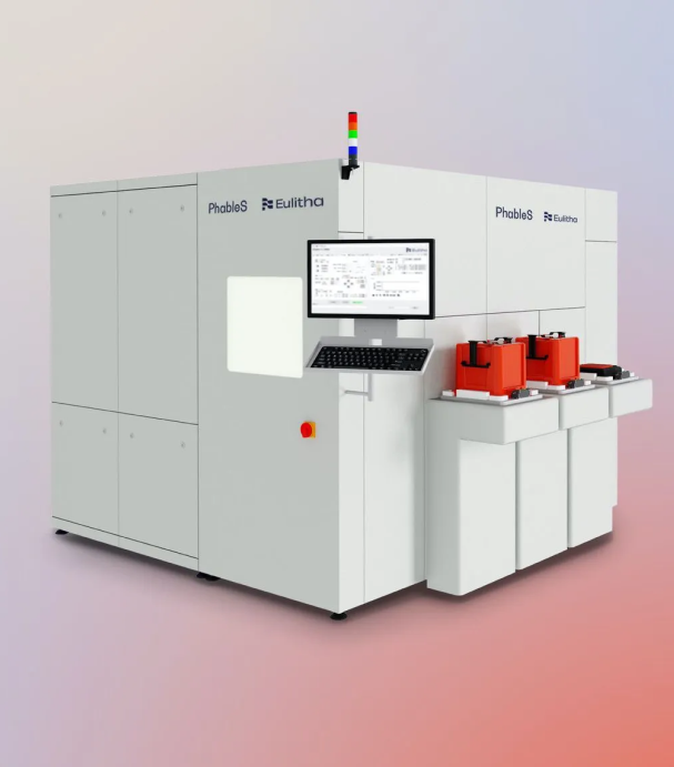
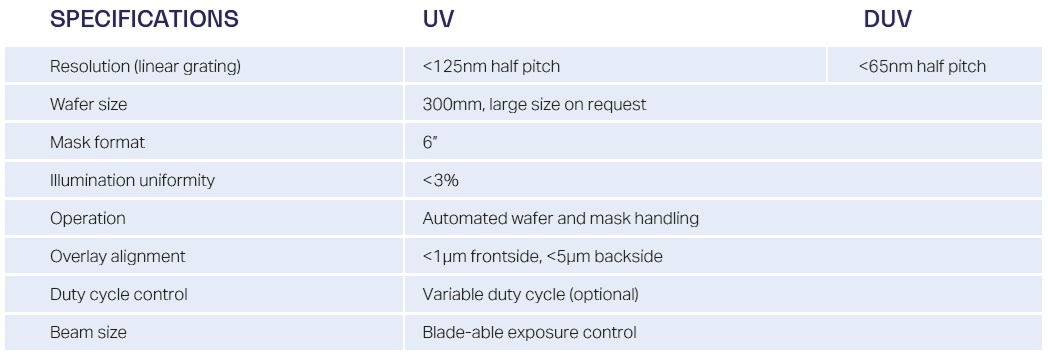
PhableS
The PhableS is a step-and-repeat lithography tool designed for larger wafer sizes, such as 200mm, 300mm, and beyond. Using the large exposure fields of displacement Talbot lithography (DTL), the PhableS tool can fill larger substrates with multiple exposures. This tool is equipped with automated wafer and mask handling within a particle-controlled environment, ideal for high-volume industrial production. It features a variable exposure field size, allowing selective printing across multiple device masks.
Applications
OPTOELECTRONICS
- DFB/DBR Lasers
- VCSEL Polarizer Gratings
- PCSEL Photonic Crystals
- Nanowire Devices
- PSS
OPTICAL COMPONENTS
- Telecom Gratings
- Anti-Reflective Surfaces
- Wire Grid (Polarizer)
- Laser Diffraction Gratings
- Spectrometer Gratings
- Sports optics – Reticles
XR (AR/VR/MR)
- Near-Eye Waveguides
- Head-Up Displays (HUD)
BIO/MEDICAL
- Bio Molecular Sensors
- X-Ray Imaging
COLOR/VISUAL EFFECTS
- Structural Colors
- Security Applications
LITHOGRAPHY SERVICES
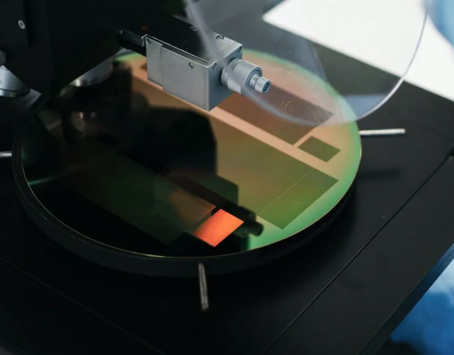
Through Eulitha's demonstration facilities in Switzerland and China, customers can access fast and innovative patterning solutions. All lithographic patterning steps are offered in-house, from the design of a photomask to the final printing in photoresist, including the provision of custom samples for various applications.
Example Products:
- AR waveguides printed according to customer design
- DFB or VCSEL gratings printed on customer wafers
- Etched silicon or quartz wafers
- Photomasks for customer DTL systems
Standard Patterns
Eulitha offers a large selection of standard patterns made upon order using its in-house photomask library.
The patterns are offered either as etched products on silicon or quartz wafers or as photoresist patterns on customer's own wafers.
DEMONSTRATION LABS
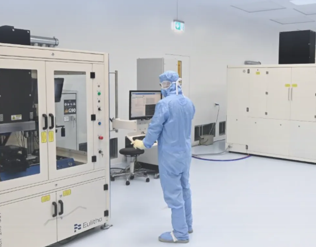
Eulitha uses its two demonstration labs in Switzerland and China to validate new photonics prototypes and applications for global customers. We aim to help customers quickly and effectively evaluate the suitability of DTL for their R&D or manufacturing needs, utilizing Eulitha's extensive expertise and equipment capabilities.
Eulitha's demo lab services enhance the development of new production processes and products with our DTL technology. This process begins by thoroughly understanding the customer's specific patterning needs. Our skilled engineering and research teams, well-versed in various applications, closely collaborate with customer teams to devise and evaluate solutions. Eulitha's partnerships with leading photoresists and mask manufacturers ensure access to cutting-edge lithography solutions.
Minimum patterning resolution down to ~60nm. Compatible with all standard and a large range of custom substrates.
